MF2003SV V-DiodeTM
应用手册
概述/特点
With advances in electronic control technology used in vehicle-mounted devices, the number of onboard Electronic Control Units (ECUs) has also increased, with applications growing increasingly diverse.
ECUs use battery or DC/DC converter output as their power source, and diodes have traditionally been used as reverse connection protection and reverse current prevention devices in the input unit. However, the increasingly large currents used in multi-functional electronic devices have raised concerns about increased diode voltage drop (VF) and heat generation, leading to demand for reverse connection protection and reverse current prevention devices that are capable of suppressing voltage drop and heat generation under high current conditions.
In response to this market demand, Shindengen has developed and launched the MF2003SV ideal diode IC (V-DiodeTM), which features a P-channel (Pch) MOSFET offering low VF, low losses, and low heat generation, together with an integrated control circuit with reverse connection protection and reverse current prevention functions.
■ Significantly reduced VF (voltage drop), losses, and heat generation.
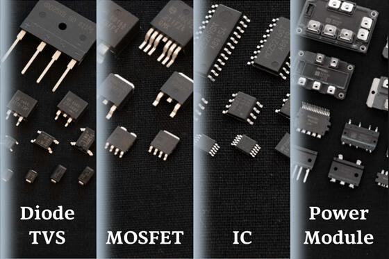
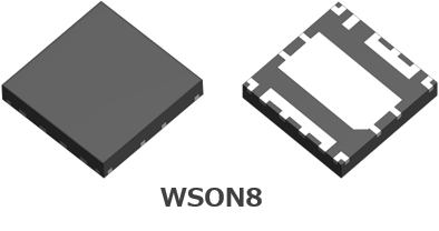
■ Compact leadless package ⇒ Contributes to reduced device size WSON8: 4mm × 4mm
■ Includes integral reverse current prevention and reverse input connection protection functions.
■ Includes integral ESD protection devices for surge protection at each pin.
■ Incorporates Pch MOSFET with active clamp function.
■ Operating voltage: 2.5V to 40V
■ Rated current: 5A
■ Internal Pch MOSFET ON resistance Ron = 53mΩ (typ), 70mΩ (max)
■ IC consumption current: max. 3uA (*at no load)
■ AEC-Q100 compliance (currently undergoing testing)
应用手册目录
1. Overview
1.1 Features
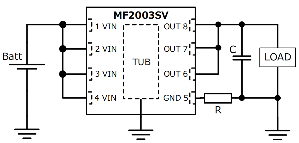
1.2 Typical circuit example
1.3 Block diagram
1.4 Pin assignment and pin functions
1.5 External appearance and dimensions (WSON8 package)
1.6 Reference soldering pads
2. Specifications
2.1 Absolute maximum ratings
2.2 Recommended operating conditions
2.3 Electrical characteristics
2.4 Reference characteristic diagrams
3. Circuit Operations and Functions
3.1 Basic operation
3.2 Startup, input drop, and shutdown operations
3.3 Load fluctuations
3.4 Reverse current prevention function
3.5 Operation for input reverse connection
3.5.1 Pch MOSFET gate control for input reverse connection
3.5.2 IC protection for input reverse connection
3.6 Internal protection devices and active clamp function
3.6.1 Overview of internal surge protection devices
3.6.2 Active clamp function operation
3.7 IC consumption current
4. Peripheral Component Selection
4.1 GND pin resistor
4.1.1 GND pin resistor R1 selection
4.1.2 Turn-on operation with addition of GND pin resistor
4.2 Capacitors close to the pins
5. Example Application Circuits
5.1 ORing connection
5.2 Parallel connection
5.3 Input surge protection
5.4 Negative output voltage protection
6. Pattern Layout
6.1 Example pattern layout
电路示例
| 应用手册免责声明 |
|
从本网站下载应用手册前,请仔细阅读以下免责声明,只有在同意的情况下,请点击"同意"按钮。 |
|