MCZ5211ST
应用手册
概述/特点
The MCZ5211ST is a frequency modulation type current resonance power supply control IC.
It features a self-startup pin (drain kick function) with a high withstand voltage of 600V for loss-free startup. It also includes a high-withstand-voltage gate driver enabling direct drive of high-side MOSFETs. Various protection functions are also included, such as overcurrent protection and out-of-resonance protection (capacitive mode protection), enabling the number of components to be reduced and efficiency increased.
Standby power improvement functions are provided (active standby function and burst function) to make it possible to maintain the power supply with high efficiency across the entire load range, making it ideal for use with the following products:
■ LED/OLED large flat-screen TV power supplies
■ Laser printer and other office equipment power supplies
■ External power supplies such as AC adapters
■ Industrial machinery power supplies
■ Isolated LED lighting power supplies
■ Audio and projector power supplies
- 600V withstand voltage self-startup pin for loss-free startup
- High-reliability 600V withstand-voltage gate driver enabling direct drive of high-side MOSFETs
- Various protection functions required for LLC converters (overcurrent, timer latch, undervoltage, overheat protection)
- Overcurrent protection function based on direct detection of resonance current in both positive and negative directions
- Capacitive mode protection function based on direct detection of resonance current in both positive and negative directions
- Support for a wide range of input voltages with 35V Vc1 withstand voltage (Vc2 UVLO 10 V/7.5 V typ.)
- MOSFET drive power supply regulator (Vc2) to ensure stable drive
- Independent separate voltage drop protection functions (UVLO) for high-side and low-side gate outputs
- Soft start function to reduce MOSFET di/dt stress
- Safety protection function to stop operation during low input voltage operation such as brown outs
- Input voltage correction function in the frequency clamp type overcurrent protection function (OCP2) corresponding to peak load, reducing stress during overloads by reducing the dependency of the overcurrent protection operation start point on the input voltage
- Two-stage switching of timer charging current during OCP2 operation to ensure safe operation at peak load for several 100ms and safety protection for the maximum peak load
- Active standby function to improve efficiency at light load
- High-efficiency burst function to improve efficiency during standby load
- Immediate latch stop function (SST pin) using external signal
- Vc1 OVP function (immediate latch stop)
- Support for 500kHz operation with control suited for higher frequencies
应用手册目录
1. Overview
1.1 Features
1.2 Block diagram
1.3 Pin assignment diagram
1.4 Pin function list
2. Basic Operations
2.1 Operating modes
2.2 Power supply section
2.3 Individual pin operation details
2.3.1 Gate driver output (VGL, VGH pins)
2.3.2 Oscillation control section (FB pin)
2.3.3 Brownout protection (Vsen pin)
2.3.4 Overcurrent protection function (CS/CSO pins)
2.3.5 OCP2 input voltage correction (CS/SSD pins)
2.3.6 Soft start, di/dt protection at startup, latch stop function (SST pin)
2.3.7 High-side driver power supply (VB pin)
2.3.8 Light load region loss improvement function (ASTBY/Burst pins)
2.3.8.1 Active standby function
2.3.8.2 Burst function
2.3.9 Overheat protection function (TSD function)
2.3.10 Vc1 overvoltage protection function (Vc1 OVP function)
2.4 Reference
3. Determining Peripheral Circuit Parameters
3.1 Input monitoring voltage section (Vsen pin)
3.2 Oscillation control section (FB pin)
3.3 Timer charge time adjustment for soft start and abnormality (SST pin)
3.4 Overcurrent protection (OCP, di/dt) point adjustment (CS pin)
3.5 Circuit constant settings when using active standby
3.6 Circuit constant settings when using burst mode
4. IC Peripheral Pattern Layout Precautions
4.1 IC peripheral pattern layout precautions
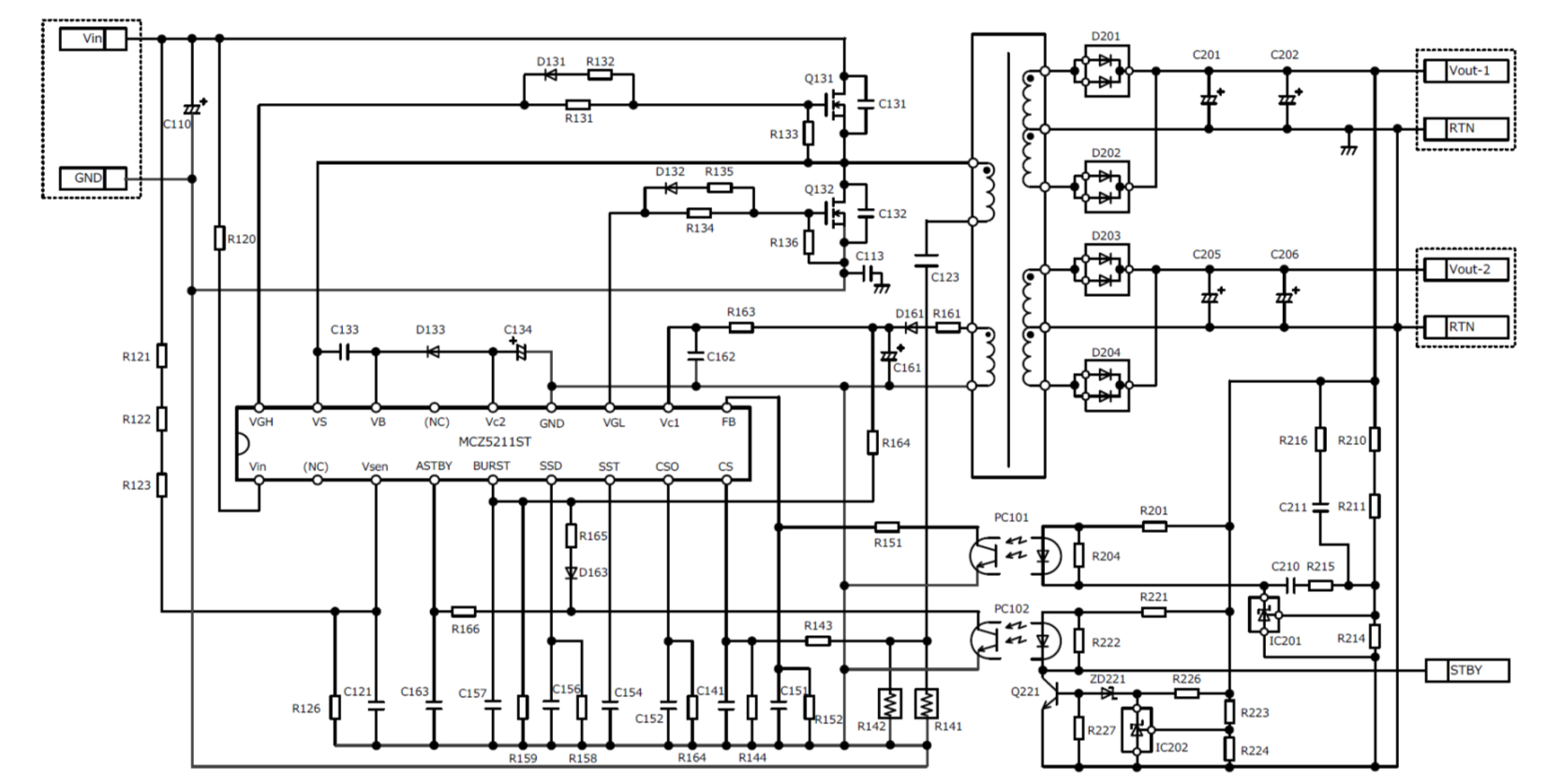
5. Circuit Examples
5.1 Typical circuit diagram
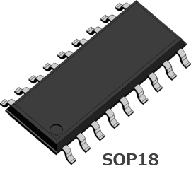
6. External Dimension Diagrams
6.1 SOP18 (MCZ5211ST)
电路示例
| 应用手册免责声明 |
|
从本网站下载应用手册前,请仔细阅读以下免责声明,只有在同意的情况下,请点击"同意"按钮。 |
|